- Published 19 Jun 2023
- Last Modified 29 Aug 2023
- 5 min
Introduction to Programmable Logic Devices
Programmable logic devices enable the functionality of electronic systems to be changed easily. Find out how in this guide.

In a standard digital electronic circuit, once a function has been wired in and programmed, it cannot be changed without being physically adjusted. However, using programmable logic devices (PLDs) means the function of a circuit isn’t fixed and can be reconfigured to perform something different without physical changes needing to be made.
This enables greater flexibility, efficiency and capabilities within digital circuits, making these integrated circuits (ICs) a popular choice for many complex electronic systems and devices.
This guide will explain the other advantages PLDs can bring to circuits, the different types available and guidance on what to keep in mind when designing them into a system.
What are Programmable Logic Devices?
Programmable logic devices (PLDs) are integrated circuits that contain a variety of logic elements which can be configured remotely by a user after installation. Typically, the logic elements include flip flops, AND and OR gates, all of which can be adjusted by a user in a software programme that’s compatible with the particular device.
This means circuits including PLDs can have one functionality when installed but be easily reprogrammed or adjusted without any physical parts of the circuit needing to be changed. To change the logic of a PLD, the right programming software and language (often referred to as a hardware description language, or HDL) must be used to ensure the correct pattern is made.
Advantages of Programmable Logic Devices
PLDs have become the IC of choice for many circuit designers even if they’re building relatively simple designs. This is for a range of reasons, including:
- Increased flexibility and adaptability in circuits, with no need to change the physical logic
- Enhanced circuit capabilities which enable designers to be more innovative and creative, even customising or personalising their designs where relevant
- Greater efficiency in terms of the space taken up on the circuit board and the amount of power used. With one IC replacing the functions of multiple devices, PLDs take up less circuit board space and are more efficient in their use of electricity
- Improved reliability due to fewer connections needing to be made on the physical circuit board and less power needing to be used, making faults less likely to occur
- Faster circuit building, with fewer elements needing to be designed and built into the circuit board and the quick adjustment of functionality via software
These various benefits are why PLDs are now the IC of choice for many designers. This makes them a viable option for many applications including telecommunications, complex control systems, and consumer electronic devices.
Types of Programmable Logic Devices
Depending on the specific requirements of a circuit, designers may choose to use a particular type of PLD. By choosing the right type, users can benefit from the programmability of some logical elements and the reliability of others that are hard-wired.
- Programmable read-only memory (PROM) devices have a fixed AND array (often used as a decoder for the input) and a programmable OR array
- Programmable logic array (PLA) devices have both a programmable AND and OR array, meaning none of its functionality is hard-wired
- Programmable array logic (PAL) devices are structured with a fixed OR array and a programmable AND array
All of these devices can be programmed to perform Boolean functions, though the specific logic of each will vary depending on which array is fixed and which is programmable. Alongside the specific logical elements of the above types, there are other forms of PLDs which are defined by their particular structures.
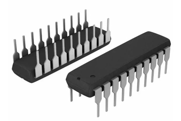
Simple Programmable Logic Devices
Simple programmable logic devices (SPLDs) are the type of PLD with the least number of gates. PLAs and PALs fall under this category. However, despite having the least complex design, they can still perform a combination of different logic and functionality. This makes them suitable for many applications including communication, digital displays and timing operations.
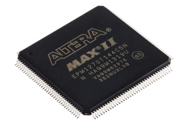
Complex Programmable Logic Devices
Complex programmable logic devices (CPLDs) are structured with blocks of macrocells that are connected together. As a result, both the individual blocks and the connections between them can be programmed separately.
With the potential for several thousand gates in a single device, the capabilities and flexibility of these programmable ICs are significant compared to simple devices.
Field Programmable Logic Devices
Field programmable logic devices (FPLDs) or field programmable gate array (FPGA) devices are structured with a programmable logic matrix, routing matrix, inputs and outputs. The programmable logic matrix is made up of two-dimensional logic blocks. The routing matrix is made up of the connections between these blocks and the input or output pins.
Finally, the programmable inputs and outputs act as buffers that can be configured to adjust the chip’s function via input, output or input-output pins.
As such, when it comes to weighing up the differences between CPLD vs FPGA devices, the main characteristic that separates them is the level of complexity, with the latter being much more programmable. Plus, the number of gates in an FPGA tends to be much higher than in a CPLD, enabling greater levels of complexity.
Designing with Programmable Logic Devices
When designing circuits using PLDs, it's important that the following process is used:
- Building out the Boolean equations that will set the inputs and define the outputs to determine how each gate will function
- Creating a logic diagram that shows how the different gates and blocks function within one PLD
- Once the logic has been designed, a design file needs to be created in the software that’s compatible with the right PLD
- Based on the design file, the performance of the gates will be simulated. This will ensure that the way the design file works is verified and accurate
- From this point, the device can be programmed according to the specific instructions in the device manual
By following these steps and choosing the right PLD for their needs, designers can make sure their circuit is working correctly and performing as intended.